- 著者
- Ken Hattori Yuya Sakai Liliany N. Pamasi Aydar Irmikimov Takaaki Higashi HaoBang Yang XiaoQian Shi FangZhun Guo Ai I. Osaka Hidekazu Tanaka Takushi Iimori Fumio Komori Azusa N. Hattori
- 出版者
- The Japan Society of Vacuum and Surface Science
- 雑誌
- e-Journal of Surface Science and Nanotechnology (ISSN:13480391)
- 巻号頁・発行日
- vol.20, no.4, pp.214-220, 2022-07-28 (Released:2022-11-26)
- 参考文献数
- 22
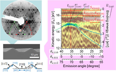
The creation of three-dimensional (3D) geometrical shapes with atomically ordered surfaces and the investigation of their physical properties are major steps contributing to the development of a new paradigm in surface science. We produced a 3D-patterned Si sample with atomically flat and reconstructed {111} facet surfaces, and investigated its structural and physical properties. To apply the conventional techniques in surface science to 3D samples with various oriented surfaces, instead of two-dimensional planar samples, an appropriate relationship between the crystallographic surface ordering on the 3D-architected surfaces and the angle-resolved photoelectron spectroscopy (ARPES) setup considering the configuration in 3D space is indispensable. The distinctive and complex low-energy electron diffraction (LEED) patterns reflecting the 3D-arranged facet surfaces showed the realization of atomically reconstructed facet surfaces on 3D-patterned Si. Surface states of the 3D-patterned Si{111} surfaces are mapped by ARPES by considering the 3D geometrical relationship. The selection of the appropriate alignment of the incident electron beam (light) for the target surfaces allows the clear observation of the band dispersion from the produced {111}7×7 facet surfaces in 3D space. Our demonstration of accessibility of ARPES technique could provide useful guidelines for new methodologies, giving a fundamental understanding of 3D-shape-induced novel functionalities.
- 著者
- Sohei Nakatsuka Taishi Imaizumi Tadashi Abukawa Azusa N. Hattori Hidekazu Tanaka Ken Hattori
- 出版者
- The Japan Society of Vacuum and Surface Science
- 雑誌
- e-Journal of Surface Science and Nanotechnology (ISSN:13480391)
- 巻号頁・発行日
- vol.19, pp.13-19, 2021-03-06 (Released:2021-03-06)
- 参考文献数
- 26
- 被引用文献数
- 2 2
Spatially arranged surfaces on the micro-rod structure, which was three-dimensionally (3D) architected on a Si(110) substrate have been thoroughly investigated by a system with micro-beam reflection high-energy electron diffraction (μ-RHEED) and scanning electron microscopy (SEM). The combination of μ-RHEED and SEM realized analytical structure investigation of 3D surfaces with the spatial resolution of sub micrometer for the 3D rectangular shaped rod consisting of a (110) top surface (20 μm wide) and {111} vertical side surfaces (10 μm wide). Exhaustive mapping revealed the peculiar reconstructed surface structures: Si(110) “16 × 2” single domain and {35 47 7} facet surfaces locally appeared on the interconnected edge region on the 3D structure in addition to the “16 × 2” and 7 × 7 super structures on flat top (110) and side {111} surfaces, respectively. The formation mechanism for “16 × 2” single-domain structure near the corner edge of the (110) surfaces and {35 47 7} facets on the corner edges between (110) and {111} surfaces were discussed from the viewpoint of the surface stability on the 3D geometrical shaped Si structure.

