27 0 0 0 OA Synthesis of Graphene-based Materials for Surface-Enhanced Raman Scattering Applications
- 著者
- Seiya Suzuki
- 出版者
- The Japan Society of Vacuum and Surface Science
- 雑誌
- e-Journal of Surface Science and Nanotechnology (ISSN:13480391)
- 巻号頁・発行日
- vol.17, pp.71-82, 2019-07-25 (Released:2019-07-25)
- 参考文献数
- 141
- 被引用文献数
- 3
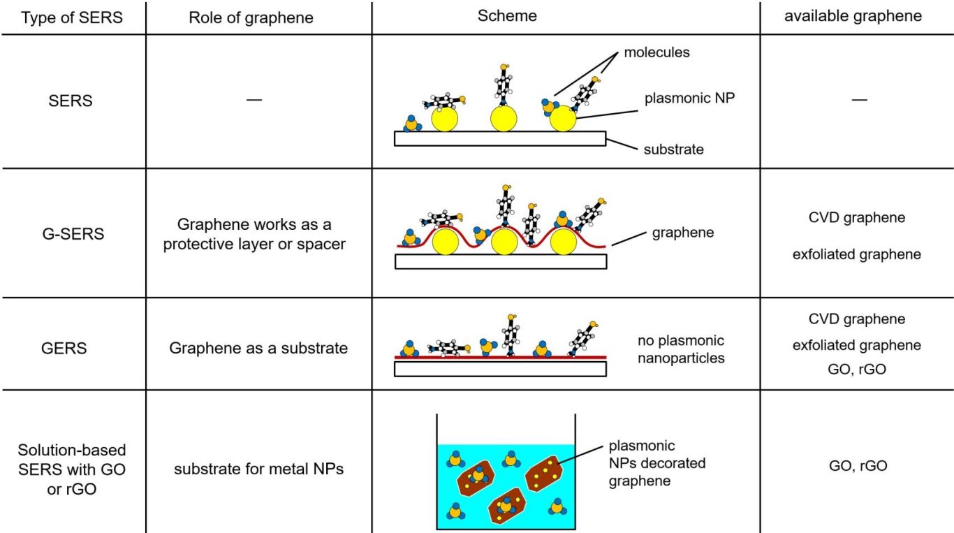
Raman spectroscopy provides a meaningful fingerprint for sensing and discriminating materials, and surface-enhanced Raman scattering (SERS) can dramatically increase Raman signals up to the single-molecule level of sensitivity. Graphene, a monolayer carbon sheet, has recently attracted considerable attention as a unique SERS substrate. However, there are various types of graphene materials, and the SERS application category is significantly correlated to the structure and quality of the graphene. This review provides a broad perspective on this research area, intended for researchers of diverse fields. First, we categorize the graphene-based SERS applications based on their structure. Second, we introduce the types of graphene (graphene oxide, reduced graphene oxide, chemical vapor deposited graphene, and carbon nanowalls) and their synthesis methods. Thereafter, we highlight state-of-the-art studies for each category of graphene-based SERS.
- 著者
- Ken Hattori Yuya Sakai Liliany N. Pamasi Aydar Irmikimov Takaaki Higashi HaoBang Yang XiaoQian Shi FangZhun Guo Ai I. Osaka Hidekazu Tanaka Takushi Iimori Fumio Komori Azusa N. Hattori
- 出版者
- The Japan Society of Vacuum and Surface Science
- 雑誌
- e-Journal of Surface Science and Nanotechnology (ISSN:13480391)
- 巻号頁・発行日
- vol.20, no.4, pp.214-220, 2022-07-28 (Released:2022-11-26)
- 参考文献数
- 22
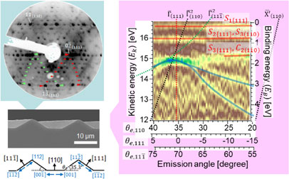
The creation of three-dimensional (3D) geometrical shapes with atomically ordered surfaces and the investigation of their physical properties are major steps contributing to the development of a new paradigm in surface science. We produced a 3D-patterned Si sample with atomically flat and reconstructed {111} facet surfaces, and investigated its structural and physical properties. To apply the conventional techniques in surface science to 3D samples with various oriented surfaces, instead of two-dimensional planar samples, an appropriate relationship between the crystallographic surface ordering on the 3D-architected surfaces and the angle-resolved photoelectron spectroscopy (ARPES) setup considering the configuration in 3D space is indispensable. The distinctive and complex low-energy electron diffraction (LEED) patterns reflecting the 3D-arranged facet surfaces showed the realization of atomically reconstructed facet surfaces on 3D-patterned Si. Surface states of the 3D-patterned Si{111} surfaces are mapped by ARPES by considering the 3D geometrical relationship. The selection of the appropriate alignment of the incident electron beam (light) for the target surfaces allows the clear observation of the band dispersion from the produced {111}7×7 facet surfaces in 3D space. Our demonstration of accessibility of ARPES technique could provide useful guidelines for new methodologies, giving a fundamental understanding of 3D-shape-induced novel functionalities.
- 著者
- Takayuki Miyamae Takashi Tokizaki
- 出版者
- 公益社団法人 日本表面科学会
- 雑誌
- e-Journal of Surface Science and Nanotechnology (ISSN:13480391)
- 巻号頁・発行日
- vol.11, pp.76-79, 2013-06-15 (Released:2013-06-15)
- 参考文献数
- 15
A near-field optical spectroscopy technique has been developed that collects the nonlinear sum-frequency signal from the surface adsorbed monolayer sample. The sum-frequency signal generated at the surface was collected with a silver-coated multi-mode fiber probe. The metal coating of the fiber effectively eliminates the far-field stray light that enters the core fiber from the outer edge, passing through the clad region. As the tip was pulled away from the sample surface, the sum-frequency signal from the GaAs crystal sample decreased rapidly with increasing tip-sample distance, indicating that the signal is essentially due to the near-field generated by the sum-frequency process. By using the metal-coated multi-mode fiber probe, information about the vibrational structure of the adsorbed molecules at the surfaces is studied. [DOI: 10.1380/ejssnt.2013.76]
- 著者
- Koji Hara Yukihiro Tominari Masakazu Yamagishi Jun Takeya
- 出版者
- The Surface Science Society of Japan
- 雑誌
- e-Journal of Surface Science and Nanotechnology (ISSN:13480391)
- 巻号頁・発行日
- vol.13, pp.426-426, 2015-09-19 (Released:2015-09-19)
- 参考文献数
- 2
On July 30th 2015, the Editor-in-Chief sent a letter to the corresponding author of the above-mentioned manuscript [1] about the result of survey by the Editorial Committee of e-J. Surf. Sci. Nanotech. According to the letter, the Committee concluded that the above-mentioned manuscript resembles the paper published in another journal [2] too much. As a result of this report, all of the authors of the above-mentioned manuscript have agreed to a complete retraction of the paper.
- 著者
- Masaharu Oshima Daisuke Mori Aki Takigawa Akihiko Otsuki Naoka Nagamura Shun Konno Yoshinobu Takahashi Masato Kotsugi Hiroshi Nohira
- 出版者
- The Japan Society of Vacuum and Surface Science
- 雑誌
- e-Journal of Surface Science and Nanotechnology (ISSN:13480391)
- 巻号頁・発行日
- vol.16, pp.257-261, 2018-06-09 (Released:2018-06-09)
- 参考文献数
- 21
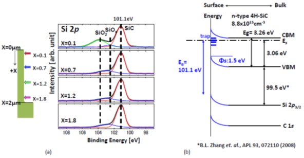
SiC trench structures having a width of 0.6 μm and a depth of 2.0 μm are fabricated by reactive ion etching (RIE) using a gas mixture of SF6, Ar, and O2. Further, SiC trench structures are cleaved to expose the sidewall for the channel region of a trench MOSFET. These structures were analyzed by pin-point photoelectron spectroscopy using a 100 nm soft-X-ray beam. It is observed that around 2 nm-thick homogeneous carbon-rich layer containing 1—2% F forms on the SiC sidewalls. This may be caused due to the re-deposition of RIE reaction products, CF4 and SiF4, under appropriate conditions to fabricate the trench walls that are approximately vertical using RIE. Further, a carbon-rich layer having a thickness of about 2.4 nm is also formed on the bottom of the SiC trench, suggesting the possibility of selective etching of Si from the SiC substrates. The position of the dominant peak that is associated with the SiC component remains constant regardless of the trench depth, suggesting homogeneous band bending due to the RIE defects, which may explain the reason for no variation being observed in the gate oxide/SiC interface trap density values. Further, the band bending of 1.50 eV that is observed on the sidewall can be attributed to a positively charged carbon vacancy (VC+). [DOI: 10.1380/ejssnt.2018.257]
- 著者
- Yuki Nagao
- 出版者
- 公益社団法人 日本表面科学会
- 雑誌
- e-Journal of Surface Science and Nanotechnology (ISSN:13480391)
- 巻号頁・発行日
- vol.10, pp.229-233, 2012-06-16 (Released:2012-06-16)
- 参考文献数
- 28
- 被引用文献数
- 1 5
In this study, contact angle measurements and an infrared p-polarized multiple-angle incidence resolution spectrometry (p-MAIRS) technique were performed on MgO(100) and quartz substrates. The contact angle and IR spectra of the in-plane and out-of-plane vibration modes depended on the cleaning methods. The surface of the as-received substrates was contaminated in MgO(100) and quartz substrates. As determined by contact angle and p-MAIR spectra analysis, plasma treatment resulted in a relatively clean and superhydrophilic surface under atmospheric conditions. [DOI: 10.1380/ejssnt.2012.229]
- 著者
- Sohei Nakatsuka Taishi Imaizumi Tadashi Abukawa Azusa N. Hattori Hidekazu Tanaka Ken Hattori
- 出版者
- The Japan Society of Vacuum and Surface Science
- 雑誌
- e-Journal of Surface Science and Nanotechnology (ISSN:13480391)
- 巻号頁・発行日
- vol.19, pp.13-19, 2021-03-06 (Released:2021-03-06)
- 参考文献数
- 26
- 被引用文献数
- 2 2
Spatially arranged surfaces on the micro-rod structure, which was three-dimensionally (3D) architected on a Si(110) substrate have been thoroughly investigated by a system with micro-beam reflection high-energy electron diffraction (μ-RHEED) and scanning electron microscopy (SEM). The combination of μ-RHEED and SEM realized analytical structure investigation of 3D surfaces with the spatial resolution of sub micrometer for the 3D rectangular shaped rod consisting of a (110) top surface (20 μm wide) and {111} vertical side surfaces (10 μm wide). Exhaustive mapping revealed the peculiar reconstructed surface structures: Si(110) “16 × 2” single domain and {35 47 7} facet surfaces locally appeared on the interconnected edge region on the 3D structure in addition to the “16 × 2” and 7 × 7 super structures on flat top (110) and side {111} surfaces, respectively. The formation mechanism for “16 × 2” single-domain structure near the corner edge of the (110) surfaces and {35 47 7} facets on the corner edges between (110) and {111} surfaces were discussed from the viewpoint of the surface stability on the 3D geometrical shaped Si structure.
- 著者
- Hikaru Horii Manaho Matsubara Kenji Sasaoka Takahiro Yamamoto
- 出版者
- The Japan Society of Vacuum and Surface Science
- 雑誌
- e-Journal of Surface Science and Nanotechnology (ISSN:13480391)
- 巻号頁・発行日
- vol.19, pp.125-130, 2021-12-23 (Released:2021-12-23)
- 参考文献数
- 40
- 被引用文献数
- 1
The thermoelectric response of bilayer graphene over a wide temperature range (0 < T ≤ 400 K) was theoretically investigated using linear response theory combined with a Green's function technique. We found that the power factor PF for a fixed chemical potential μ exhibits a maximum at a certain T. On the other hand, we found that the PF for a fixed T exhibits a maximum (PFmax) at an optimal μ [or optimal carrier concentration (nopt)]. In addition, we clarified the T dependence of nopt and PFmax and explained the existence of nopt in terms of the thermal excitation of electrons between the valence and conduction bands, which cannot be predicted by the conventional Mott formula.
- 著者
- Kenichi Ozawa Susumu Yamamoto Kazuhiko Mase Iwao Matsuda
- 出版者
- The Japan Society of Vacuum and Surface Science
- 雑誌
- e-Journal of Surface Science and Nanotechnology (ISSN:13480391)
- 巻号頁・発行日
- vol.17, pp.130-147, 2019-09-07 (Released:2019-09-07)
- 参考文献数
- 89
- 被引用文献数
- 10
Establishing an accurate view of the photocatalytic mechanism of titanium dioxide (TiO2) has been a challenging task since the discovery of the Honda-Fujishima effect. Despite the great success of catalytic studies in elucidating the chemical and physical aspects of photocatalysis, many questions remain. A surface science approach, which is characterized by the use of atomically well-defined surfaces in precisely controlled environments, is a powerful tool to shed light on the fundamental mechanism, especially the dynamics of photoexcited carriers. In the present contribution, recent progress in photocatalytic research that correlates photocatalytic activity and carrier dynamics on rutile and anatase TiO2 is reviewed. A special focus is placed on the lifetime of photoexcited carriers. We present a method to determine the carrier lifetime; pump-probe time-resolved soft X-ray photoelectron spectroscopy, utilizing an ultraviolet laser as a pump light and a synchrotron radiation as a probe light. The carrier lifetime is found to be linearly correlated with the photocatalytic decomposition/desorption rate of acetic acid adsorbed on single-crystal TiO2 surfaces. The important role of a potential barrier on the TiO2 surface, which influences the carrier lifetime and the photocatalytic activity, is discussed.
2 0 0 0 OA Adsorption and Diffusion Properties of a Single Iron Atom on Light-Element-Doped Graphene
- 著者
- Shun Hasegawa Yuji Kunisada Norihito Sakaguchi
- 出版者
- The Japan Society of Vacuum and Surface Science
- 雑誌
- e-Journal of Surface Science and Nanotechnology (ISSN:13480391)
- 巻号頁・発行日
- vol.16, pp.193-200, 2018-05-25 (Released:2018-05-25)
- 参考文献数
- 38
- 被引用文献数
- 4
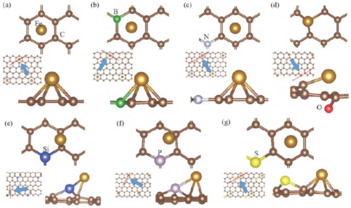
In this study, we calculated the diffusion of an Fe atom on graphene and various light-element (B, N, O, Si, P, and S)-doped graphene supports, using first-principles calculations based on density functional theory. We focused on dopants that could suppress the detachment and diffusion of an Fe atom. Such doped graphene supports would have strong potential in high-durability fuel cell catalysts and hydrogen storage materials. The Fe atom adsorbs on pristine graphene via ionic bonding. The bonding between the Fe atom and pristine graphene is very weak, and it has a low adsorption energy of −0.61 eV. Doped graphene contains unoccupied localized orbitals. B-, O-, Si-, and P-doped graphene show high adsorption energies of −1.70 eV, −2.70 eV, −1.46 eV, and −1.38 eV, respectively. Thus, these graphene supports could suppress the detachment of Fe nanoclusters and nanoparticles. We demonstrate that these doped graphene supports with high adsorption energies also have high diffusion barriers, which suppresses the agglomeration of Fe nanoclusters and nanoparticles. We conclude that B-, O-, Si-, and P-doped graphene are promising supports for enhancing the adsorption lifetime of Fe nanoclusters and nanoparticles. [DOI: 10.1380/ejssnt.2018.193]
2 0 0 0 OA Retraction: Organic Single-Crystal Transistors with Secondary Gates on Source and Drain Electrodes
- 著者
- Koji Hara Yukihiro Tominari Masakazu Yamagishi Jun Takeya
- 出版者
- The Japan Society of Vacuum and Surface Science
- 雑誌
- e-Journal of Surface Science and Nanotechnology (ISSN:13480391)
- 巻号頁・発行日
- vol.6, pp.138-141, 2008-05-29 (Released:2008-05-29)
- 参考文献数
- 10
This article was retracted.
- 著者
- Stephen Matthew Lyth Yuta Nabae Nazrul Md. Islam Teruaki Hayakawa Shigeki Kuroki Masa-aki Kakimoto Seizo Miyata
- 出版者
- 公益社団法人 日本表面科学会
- 雑誌
- e-Journal of Surface Science and Nanotechnology (ISSN:13480391)
- 巻号頁・発行日
- vol.10, pp.29-32, 2012-03-10 (Released:2012-03-10)
- 参考文献数
- 40
- 被引用文献数
- 5 18 6
Graphene is ideally suited to electrochemistry by virtue of its high surface area and impressive electronic properties. Nitrogen incorporation can be used to tailor the properties of graphene. Here we present a simple solvothermal technique to produce a nitrogen-containing foam-like macroporous graphene powder doped with up to 15 wt% nitrogen. This is applied as an effective non-precious, metal-free electrochemical catalyst for oxygen reduction in acid media. [DOI: 10.1380/ejssnt.2012.29]
- 著者
- Kiyoshi Urakawa Motohiro Kasuya Kiyoshi Kanie Hiroyuki Shibata Takenobu Sato Takashi Ebata Shigeru Suzuki
- 出版者
- The Japan Society of Vacuum and Surface Science
- 雑誌
- e-Journal of Surface Science and Nanotechnology (ISSN:13480391)
- 巻号頁・発行日
- pp.2022-026, (Released:2022-06-11)
- 参考文献数
- 16
- 被引用文献数
- 2
The aluminum oxide thin films formed on the surfaces of FeCo-V alloys doped with a small amount of aluminum were characterized by ellipsometry and electrical resistivity measurements. Aluminum oxide films on alloy surfaces were selectively formed by annealing under a low partial pressure of oxygen. The thickness of the oxide films increased with increasing aluminum content and temperature. However, the electrical resistivity of the oxide thin films did not correlate with the thickness of the oxide films. To clarify the anomaly of the resistivity, micro-beam X-ray photoelectron spectroscopy (XPS) was used to characterize the two-dimensional distribution of elements on the alloy surface. The XPS results show that the oxide films were partially exfoliated in the alloys with a high aluminum content. In particular, the oxide films were likely to be exfoliated or separated in relatively thick oxide films because of their dissimilar properties at vicinities close to the interface between the substrate and aluminum oxide thin films. Therefore, the thickness of the oxide film, and the amount of aluminum, are crucial for controlling the formation of aluminum oxide thin films with high resistivity in FeCo-V alloys.
- 著者
- Shinya Hosokawa Naohisa Happo Kouichi Hayashi Tomohiro Matsushita Aichi Yamashita
- 出版者
- The Japan Society of Vacuum and Surface Science
- 雑誌
- e-Journal of Surface Science and Nanotechnology (ISSN:13480391)
- 巻号頁・発行日
- pp.2022-001, (Released:2022-01-29)
- 参考文献数
- 26
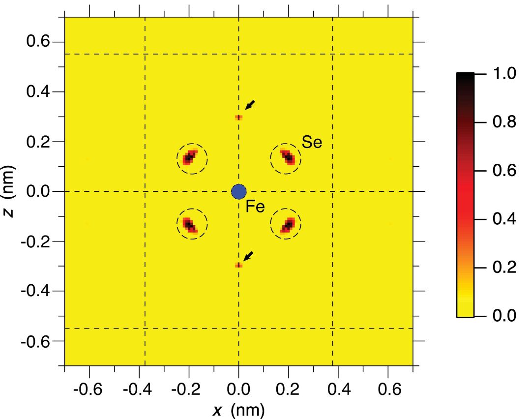
Fe Kα X-ray fluorescence holography measurements were carried out at room temperature on an FeSe high-temperature superconductor to clarify the relationship between the local structures around the Fe atoms and the superconducting nature. The obtained three-dimensional atomic arrangements strongly reveal a formation of strong FeSe4 clusters. On the other hand, the Se—Fe—Se bond angle largely spreads, causing a large ambiguity in the chalcogen height and large displacements of the Fe sublattice. Thus, it is reasonable that the tetragonal-to-orthorhombic structural (nematic) transition does not affect the magnetic ordering in the Fe layer.
- 著者
- Hirotaka Asai Takayuki Tanaka Hidekazu Murata Eiji Rokuta
- 出版者
- The Japan Society of Vacuum and Surface Science
- 雑誌
- e-Journal of Surface Science and Nanotechnology (ISSN:13480391)
- 巻号頁・発行日
- vol.19, pp.131-142, 2021-12-28 (Released:2021-12-28)
- 参考文献数
- 47
The surface diffusion method was used to produce tungsten (W) nanopyramids coated with monolayer films of platinum (Pt) and gold (Au). Although the general structures of the nanopyramids were the same, the top of the nanopyramids was different from the Pt and Au cases, i.e., a monomer was observed for Pt, whereas a trimer observed for Au. The effects of simultaneous heating and the electric field on the structural evolution of nanopyramids were also studied. We observed that the broken nanopyramids were rapidly regenerated by heating in an electric field. The opening angles of field-emitted electrons were found to be approximately ±2° and ±2.5° for Pt and Au, respectively. From the obtained results, it was observed that the field-emission properties of all specimens were almost the same.
- 著者
- Federico Grillo Rory Megginson Jenny Christie Stephen M. Francis Neville V. Richardson Christopher J. Baddeley
- 出版者
- The Japan Society of Vacuum and Surface Science
- 雑誌
- e-Journal of Surface Science and Nanotechnology (ISSN:13480391)
- 巻号頁・発行日
- vol.16, pp.163-171, 2018-05-19 (Released:2018-05-19)
- 参考文献数
- 77
- 被引用文献数
- 8 9
The structure and surface chemistry of ultrathin metallic films of one metal on another are strongly influenced by factors such as lattice mismatch and the formation of near-surface alloys. New morphologies may result with modified chemical properties which in turn open up different routes for molecular adsorption, desorption and surface functionalization, with important consequences in several fields of application. The Cu/Au(111) system has received the attention of many studies, only a few however have been performed in ultra-high vacuum (UHV), using surface sensitive techniques. In this contribution, the room temperature deposition of copper onto the (22×√3)-Au(111) surface, from submonolayer to thick film, is investigated using scanning tunnelling microscopy (STM). The onset of copper adsorption is seen to occur preferentially at alternate herringbone elbows, with a preference for hcp sites. With increasing coverage, copper-rich islands exhibit a reconstructed surface reminiscent of the clean Au(111) herringbone reconstruction. Disordered, pseudo-ordered and ordered surface layers are observed upon annealing. Models for the initial adsorption/incorporation mechanism, formation of adlayers and evolution with increasing coverage and annealing are qualitatively discussed. Further, the reactivity of copper-doped Au(111) systems is considered towards the adsorption of organic molecules of interest in nanotechnology and in catalytic applications. [DOI: 10.1380/ejssnt.2018.163]
- 著者
- Takanori Koitaya Susumu Yamamoto Iwao Matsuda Jun Yoshinobu
- 出版者
- The Japan Society of Vacuum and Surface Science
- 雑誌
- e-Journal of Surface Science and Nanotechnology (ISSN:13480391)
- 巻号頁・発行日
- vol.17, pp.169-178, 2019-11-02 (Released:2019-11-02)
- 参考文献数
- 86
- 被引用文献数
- 4 13
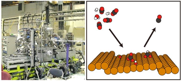
In-situ analysis of heterogeneous catalysts under reaction condition is indispensable to understand reaction mechanisms and nature of active sites. Ambient-pressure X-ray photoelectron spectroscopy (AP-XPS) is one of the powerful methods to investigate chemical states of catalysts and reaction intermediates adsorbed on the surface. In this review, reaction of carbon dioxide on Cu(997) and Zn-deposited Cu(997) surfaces are discussed as an example of surface chemistry of weakly adsorbed molecules, together with a brief overview of recent progress in AP-XPS methods.
- 著者
- Tsuneo Fukuda Ippei Kishida
- 出版者
- The Japan Society of Vacuum and Surface Science
- 雑誌
- e-Journal of Surface Science and Nanotechnology (ISSN:13480391)
- 巻号頁・発行日
- vol.19, pp.112-118, 2021-11-11 (Released:2021-11-11)
- 参考文献数
- 29
- 被引用文献数
- 2
First-principles total-energy calculations were applied to 0 to 1 ML of silicon-embedded Ni(100) surfaces in the outmost layer within a 2 × 4 unit cell. Up to a half monolayer of embedded silicon, the surface energy decreased monotonically with increasing the number of embedded silicon, and the lowest energy structure was a √2 × √2-R45° [or c(2 × 2)] structure with diagonally aligned embedded silicon of 0.5 ML. Beyond the half monolayer, the surface energy increased with increasing the number of embedded silicon. The energy of the silicon-embedded structure in the outmost layer of the Ni(100) surface was compared with silicon embedded in the second layer and silicon adsorbed on the Ni(100) surface. Both configurations gave higher energies, which shows the robustness of the √2 × √2-R45° structure on the Ni(100) surface. The present results are in perfect agreement with our recent report [T. Fukuda et al., Jpn. J. Appl. Phys. 59, 065501 (2020)].
1 0 0 0 OA Mechanism of Oxygen Reduction Reaction on Monolayer WTe2 with and without S Dopant at Low Coverage
- 著者
- Do Ngoc Son Viorel Chihaia Pham Tan Thi
- 出版者
- The Japan Society of Vacuum and Surface Science
- 雑誌
- e-Journal of Surface Science and Nanotechnology (ISSN:13480391)
- 巻号頁・発行日
- vol.19, pp.119-124, 2021-11-13 (Released:2021-11-13)
- 参考文献数
- 31
Transition metal dichalcogenides possess properties such as low cost, easy fabrication, and suitability for various applications. Monolayer WTe2 is a potential electro-catalytic material for the oxygen reduction reaction (ORR). However, the reaction mechanism on pure and S-doped monolayer WTe2 remains unknown; therefore, this work is devoted to clarifying the current topic using density functional theory calculations and a thermodynamics model. We found that the ORR mechanism is a four-electron pathway on pure and S-doped monolayer WTe2. However, S-doped monolayer WTe2 increases the thermodynamic barrier of the ORR compared to pure monolayer WTe2. Therefore, the S dopant decreases the performance of WTe2. The result implies that doping with different elements is not always a method to improve the efficiency of chemical reactions.
- 著者
- Afif Hamzens Ridho Kurniawan Damar Rastri Adhika Widayani Ahmad Nuruddin
- 出版者
- The Japan Society of Vacuum and Surface Science
- 雑誌
- e-Journal of Surface Science and Nanotechnology (ISSN:13480391)
- 巻号頁・発行日
- vol.19, pp.1-8, 2021-02-27 (Released:2021-02-27)
- 参考文献数
- 31
- 被引用文献数
- 2
A near-infrared (NIR) reflector in cotton clothes may prevents several dermatological problems. TiO2 is commonly used for the NIR reflector coating in cotton. The NIR reflectance value is expected to increase if smaller TiO2 particles were used. A simple mechanical process of ultrasonic wet-milling to reduce the TiO2 particle size is proposed in this study. The reduction process utilizes ultrasonic cavitation by an ultrasonic homogenizer has succeeded in reducing the particle size from 170 to 80 nm as indicated by particle size measurement results and as supported by transmission electron microscopy results. The wet-milling particles of 80 nm TiO2, along with 170 and 280 nm TiO2, were used to coat cotton fabrics. Optimization of the coating process was performed using citric acid and chitosan as binder agents. The effect of citric acid and chitosan was studied through NIR spectroscopy, scanning electron microscopy, and X-ray fluorescence. From the NIR spectroscopy characterization results, it is found that the fabrics which are coated with the smallest TiO2 particle size (80 nm) indeed show highest NIR reflectance among others.
