1 0 0 0 OA 電解複合研磨による金属の超鏡面化技術
1 0 0 0 RFバイアススパッタリングによるシリコン酸化膜
- 著者
- 江口 剛治 桜井 弘美 原田 曠嗣 柏木 忠
- 出版者
- The Vacuum Society of Japan
- 雑誌
- 真空 (ISSN:05598516)
- 巻号頁・発行日
- vol.27, no.10, pp.759-767, 1984
Silicon oxide films have been formed by a RF bias sputter-deposition system using a quartz target in Ar or Ar/O<SUB>2</SUB> sputtering gas. Substrate bias voltage <I>V</I><SUB>b</SUB> was varied from 0 to-200 V, at the total power of 1.9 W/cm<SUP>2</SUP>.<BR>In order to evaluate the planarization effect, the step coverage of the film on AlSi patterns was examined by SEM and compared with the computer simulated profiles using the Lehmann's method, and a good agreement was obtained. Further, we have applied this planarization technology to a 6-level metallization and realized the good step coverage.<BR>The properties of the silicon-oxide films were also studied. In the case of the Ar gas sputtering, the leakage current and the compressive stress in the film increase with increasing <I>V</I><SUB>b</SUB>. It is found that the Ar/O<SUB>2</SUB> gas sputtering improves the film properties of both the inner stress and leakage current. Auger analysis indicates that the films deposited in Ar/O<SUB>2</SUB> gas have O/Si ratio of about 2, but O/Si ratio of the films deposited in Ar gas is less than 2. From these data, the improvement of the properties of the films can be explained as following; oxygen in Si-O network in the films is removed by Ar ion bombardment during bias sputtering, and damaged bond is compensated by oxygen addition.
1 0 0 0 OA イオンビーム誘起化学蒸着法による酸化スズ薄膜の作製
- 著者
- 藤川 友佳 木内 正人 松谷 貴臣 竹内 孝江
- 出版者
- 一般社団法人 日本真空学会
- 雑誌
- 真空 (ISSN:05598516)
- 巻号頁・発行日
- vol.49, no.12, pp.780-781, 2006 (Released:2007-08-09)
- 参考文献数
- 7
We deposited transparent and electrical conductive thin films on polymer substrates ZEONOR® (cycloolefin) by oxygen ion beam induced chemical vapor deposition (IBICVD) with tetramethylstannane (TMS). The film depositions were carried out the acceleration voltage of oxygen ion beam in range from 50 to 300 eV. The deposition time was fixed at 180 minutes at all conditions. Under irradiation of 300 eV oxygen ions, the optical transmittance at 550 nm and the resistivity of the prepared film were 80% and 5.4×10⁻² Ω•cm, respectively. When oxygen ion energy increased from 50 to 300 eV, root mean square of roughness and contamination of carbon were decreased.
1 0 0 0 OA 酸化チタン光触媒薄膜の内部応力と光分解活性に関する研究
- 著者
- 宮村 会実佳 金田 健志 佐藤 泰史 重里 有三
- 出版者
- 一般社団法人 日本真空学会
- 雑誌
- 真空 (ISSN:05598516)
- 巻号頁・発行日
- vol.50, no.6, pp.432-436, 2007 (Released:2008-01-01)
- 参考文献数
- 13
Photocatalytic activities of titanium dioxide (TiO2) films deposited by rf sputtering were investigated from view points of their internal stress. TiO2 films were deposited on fused quartz glass or 100 μm thick micro-sheet glass substrates at room temperature, 200 or 400°C under various total gas pressures (Ptot) of 0.3~5.0 Pa with oxygen flow ratio [O2/(O2+Ar)] of 60% using a Ti metal target. Photocatalytic activity was evaluated by photodecomposition of acetaldehyde (CH3CHO) under UV illumination (black light lamp, 0.4 mW/cm2). Compressive internal stress was estimated by cantilever method using the micro-sheet glass, which clearly decreased from -2.1 to -0.1 GPa with the increase in the Ptot from 0.3 to 3.0 Pa. The films with the compressive stress less than -0.5 GPa performed the photocatalytic activity. Furthermore, compressive or tensile stress was applied by external force on the TiO2 films deposited on the curved micro sheet glasses by flattening these substrates after the deposition. The photodecomposition activity of the films with the slight compressive stress improved clearly, whereas the one of the films with the tensile stress degraded.
1 0 0 0 OA 質量分析計の検出器—二次電子増倍管
- 著者
- 大村 孝幸 山口 晴久
- 出版者
- 一般社団法人 日本真空学会
- 雑誌
- 真空 (ISSN:05598516)
- 巻号頁・発行日
- vol.50, no.4, pp.258-263, 2007 (Released:2008-01-01)
- 参考文献数
- 13
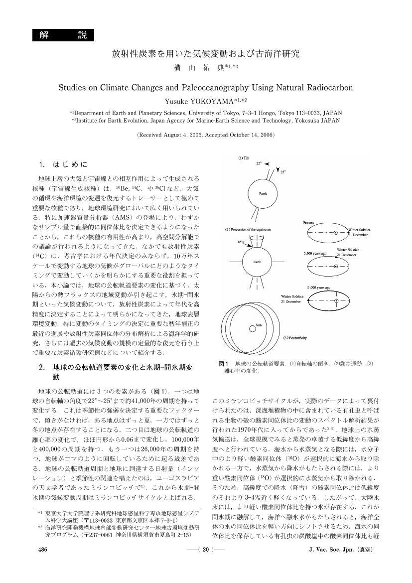
1 0 0 0 OA 放射性炭素を用いた気候変動および古海洋研究
- 著者
- 横山 祐典
- 出版者
- 一般社団法人 日本真空学会
- 雑誌
- 真空 (ISSN:05598516)
- 巻号頁・発行日
- vol.50, no.7, pp.486-493, 2007 (Released:2008-01-01)
- 参考文献数
- 66
- 被引用文献数
- 1 1
- 著者
- 森田 清三 杉本 宜昭 大藪 範昭 クスタンセ O. 阿部 真之 ポウ P. ジェリネク P. ペレッツ R.
- 出版者
- The Vacuum Society of Japan
- 雑誌
- 真空 (ISSN:05598516)
- 巻号頁・発行日
- vol.50, no.3, pp.181-183, 2007-03-20
An atomic force microscope (AFM) under noncontact and nearcontact regions operated at room-temperature (RT) in ultrahigh vacuum, is used as a tool for topography-based atomic discrimination and atomic-interchange manipulations of two intermixed atomic species on semiconductor surfaces. Noncontact AFM topography based site-specific force curves provide the chemical covalent bonding forces between the tip apex and the atoms at the surface. Here, we introduced an example related to topography-based atomic discrimination using selected Sn and Si adatoms in Sn/Si(111)-(√3 ×√3 ) surface. Recently, under nearcontact region, we found a lateral atom-interchange manipulation phenomenon at RT in Sn/Ge(111)-c(2×8) intermixed sample. This phenomenon can interchange an embedded Sn atom with a neighbor Ge atom at RT. Using the vector scan method under nearcontact region, we constructed "Atom Inlay", that is, atom letters "Sn" consisted of 19 Sn atoms embedded in Ge(111)-c(2×8) substrate. Using these methods, now we can assemble compound semiconductor nanostructures atom-by-atom.<br>


